


 By
By Every time a generative model writes a block of code, an autonomous vehicle avoids a collision, or an enterprise searches through millions of internal records in seconds, physical silicon does the heavy lifting. While headlines focus on foundation models and chatbot interfaces, artificial intelligence is anchored in physical hardware: billions of microscopic transistors switching trillions of times per second inside specialized AI chips.
For decades, computing power grew predictably along Moore’s Law and Dennard scaling. General-purpose processors steadily improved, handling whatever software developers built. But the rise of modern deep learning shattered that computational model. Neural networks do not run software like web browsers or operating systems do. Instead, they process massive amounts of linear algebra, executing trillions of simultaneous matrix multiplications across vast arrays of numbers.
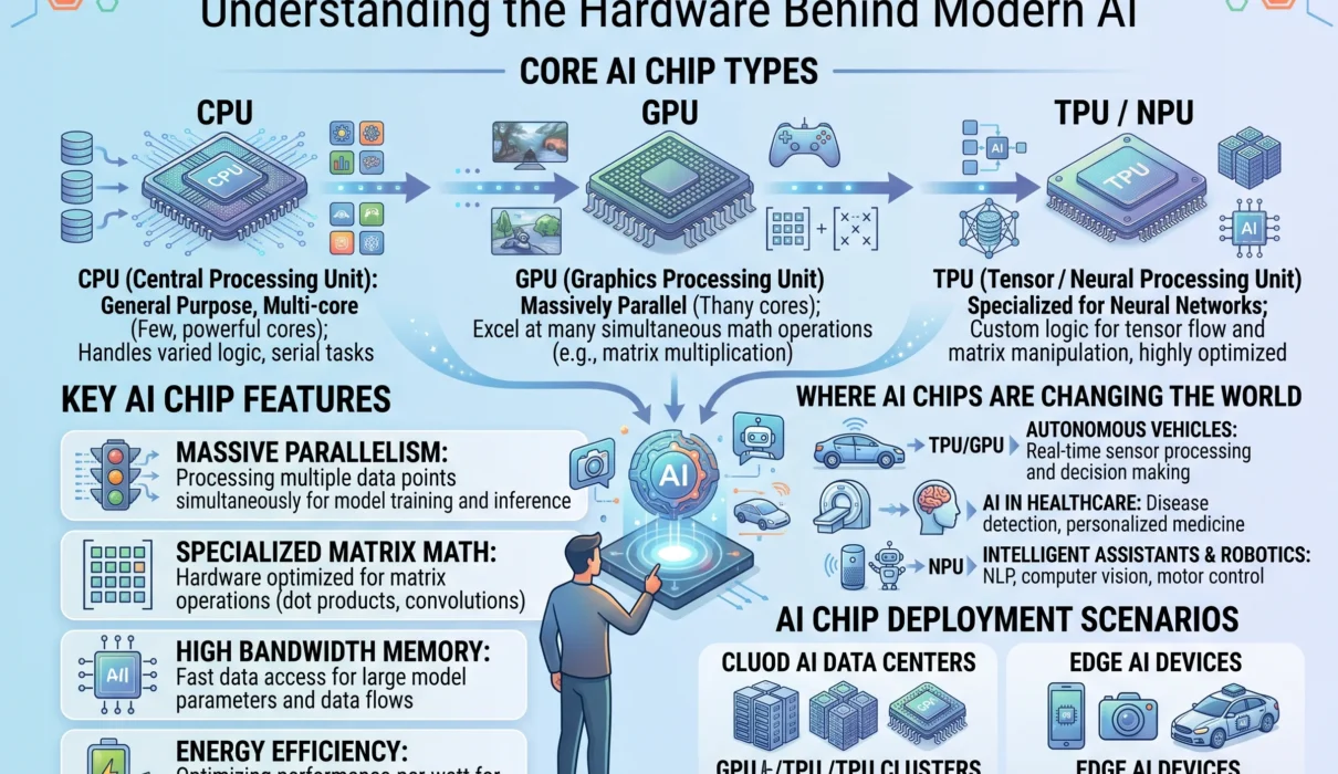
Attempting to run these models on traditional general-purpose processors wastes power and causes severe latency bottlenecks. To address this, the semiconductor industry has shifted toward specialized AI processors, purpose-built machine learning hardware, and novel semiconductor technology architectures.
1. What Is an AI Chip?
At its most fundamental level, an AI chip (frequently termed an AI accelerator) is a silicon processor specifically designed and optimized to execute the mathematical primitives of artificial neural networks.
Unlike traditional Central Processing Units (CPUs) engineered to execute complex, branch-heavy instructions one after another, an AI accelerator is built for massive parallel throughput and streamlined matrix mathematics.
TRADITIONAL CPU ARCHITECTURE vs. AI ACCELERATOR ARCHITECTURE

  CPU (Control-Heavy, Sequential)        AI CHIP (Compute-Dense, Parallel)
  ┌─────────────────────────────────┐    ┌─────────────────────────────────┐
  │  Control Logic & Branch Pred.   │    │ Control │ L1 Cache │ Control    │
  ├───────────┬───────────┬─────────┤    ├─────────┴──────────┴────────────┤
  │ Core 1    │ Core 2    │ Core 3  │    │ [PE] [PE] [PE] [PE] [PE] [PE]   │
  ├───────────┴───────────┴─────────┤    │ [PE] [PE] [PE] [PE] [PE] [PE]   │
  │ Massive L3 Cache SRAM Pools     │    │ [PE] [PE] [PE] [PE] [PE] [PE]   │
  ├─────────────────────────────────┤    │ Thousands of Processing Elements│
  │ High-Latency DRAM Interface     │    ├─────────────────────────────────┤
  └─────────────────────────────────┘    │ High-Bandwidth Memory (HBM) Bus │
                                         └─────────────────────────────────┘
The mathematical foundation of deep learning consists predominantly of GEMM (General Matrix Multiply) operations and convolutions. A single transformer layer in a large language model takes an input activation vector, multiplies it against a multi-billion-parameter weight matrix, applies an activation function, and repeats the process across dozens of layers:
$$\mathbf{Y} = \text{Activation}(\mathbf{W} \cdot \mathbf{X} + \mathbf{b})$$
Where conventional microprocessors spend substantial silicon real estate on out-of-order execution, speculative branching, and deep cache hierarchies to make single-threaded execution fast, an AI chip strips away that overhead. Instead, it dedicates its surface area to thousands of dense arithmetic logic units (ALUs), fused multiply-accumulate (MAC) units, and high-speed memory interfaces that calculate matrix transformations in parallel.
2. Training vs. Inference: Two Radically Different Hardware Demands
One of the most critical distinctions in machine learning hardware is the difference between training an AI model and performing inference. A chip optimized for one task is often ill-suited for the other.
                 THE MACHINE LEARNING LIFECYCLE ON SILICON

  TRAINING (Model Creation)                 INFERENCE (Model Execution)
  ┌────────────────────────────────────┐    ┌────────────────────────────────────┐
  │ Forward Pass ──► Error Calculation │    │ Input Prompt / Sensor Ingestion    │
  │ Backward Pass (Gradient Descent)   │    │ Single Forward Pass Only           │
  │ Weight Updates across Cluster      │    │ Generates Next Token / Classifies  │
  ├────────────────────────────────────┤    ├────────────────────────────────────┤
  │ • Massive 16-bit/8-bit Floating Pt │    │ • Low-Precision Math (INT8, INT4)  │
  │ • Giant Memory Capacity (HBM)      │    │ • Memory-Bandwidth Constrained     │
  │ • Ultra-Fast Interconnects (RoCE)  │    │ • Optimized for Low Latency / Watt │
  │ • Multi-Megawatt Data Centers      │    │ • Deployed at Cloud & Edge/Devices │
  └────────────────────────────────────┘    └────────────────────────────────────┘
The Training Phase: Maximum Throughput and Memory Capacity
Training is the process of creating an AI model from scratch or fine-tuning a foundational checkpoint on raw datasets.
- The Math: The system processes data through a forward pass, calculates an error metric (loss function), executes backpropagation via the chain rule to calculate mathematical gradients, and updates model weights.
- Hardware Demands: Training requires high numerical dynamic range (typically FP16, BF16, or FP8 floating-point precision) to prevent gradients from vanishing or exploding. It demands immense memory capacity and bandwidth to store model weights, optimizer states (such as Adam), and activation caches.
- Scale: Training frontier models requires thousands of chips operating as a single unified supercomputer connected by high-speed networking fabrics, consuming megawatts of power for weeks or months.
The Inference Phase: Low Latency, High Efficiency, and Token Decode
Inference is what happens when a user interacts with an already-trained model—such as submitting a prompt to generate text, running facial recognition on a smartphone, or processing live sensor frames in an industrial camera.
- The Math: Inference requires only a forward pass. Weights are static and frozen; there are no backward passes, gradient calculations, or optimizer updates.
- Hardware Demands: Efficiency, latency, and operational cost take priority. Inference hardware frequently leverages aggressive quantization, converting 16-bit floating-point weights down to 8-bit (INT8) or 4-bit (INT4) integers. This reduces memory footprint by 50% to 75% without compromising output quality, allowing models to run on smaller silicon footprints with minimal energy draw.
- The Memory-Bound Challenge: During auto-regressive text generation, language models output one token at a time. The processor must load every single model parameter from memory into its compute cores for each token produced. As a result, inference performance is often throttled not by raw compute power, but by memory bandwidth—the speed at which data travels from memory to arithmetic units.
3. The AI Processor Landscape: GPUs, TPUs, ASICs, and FPGAs
The term “AI chip” does not denote a single, monolithic design. Instead, it encompasses a spectrum of hardware architectures, each balancing flexibility against efficiency.
                     FLEXIBILITY vs. EFFICIENCY SPECTRUM

   High Flexibility                                      Maximum Efficiency
   ◄──────────────────────────────────────────────────────────────────────►
        CPU               GPU               FPGA             ASIC / TPU
   General Code     Parallel Graphic   Field-Programmable    Fixed Silicon
    Branching         & Matrix Math       Logic Gates         Single-Task
  (Universal OS)      (CUDA Stack)     (Low Latency Fin.)    (Scale LLMs)
┌────────────────────────────────────────────────────────────────────────┐
│                   AI HARDWARE ARCHITECTURE MATRIX                      │
├─────────────┬──────────────────────────┬───────────────────────────────┤
│ Chip Type   │ Core Strengths           │ Ideal AI Use Cases            │
├─────────────┼──────────────────────────┼───────────────────────────────┤
│ GPU         │ Massive software support │ Frontier model training,      │
│             │ (CUDA), high parallel    │ multimodal generation,        │
│             │ throughput, flexibility  │ dynamic model experimentation │
├─────────────┼──────────────────────────┼───────────────────────────────┤
│ ASIC / TPU  │ Maximum energy efficiency│ Scaled cloud inference, large-│
│             │ and price-performance    │ scale static model training,  │
│             │ for defined math ops     │ hyperscale cost-reduction     │
├─────────────┼──────────────────────────┼───────────────────────────────┤
│ NPU         │ Low power (2W–15W),      │ On-device edge processing,    │
│             │ compact silicon area,    │ mobile photography, always-on │
│             │ zero-copy unified memory │ voice and camera features     │
├─────────────┼──────────────────────────┼───────────────────────────────┤
│ FPGA        │ Reconfigurable logic,    │ High-frequency trading,       │
│             │ deterministic latency,   │ aerospace, rapid hardware     │
│             │ zero-mask tapeout cost   │ prototyping, telecom (5G/6G)  │
└─────────────┴──────────────────────────┴───────────────────────────────┘
1. GPUs (Graphics Processing Units): The Industry Standard
Originally engineered to compute 3D polygons and pixel shaders for computer graphics, GPUs became the foundation of the AI revolution when researchers realized that rendering graphics and computing neural networks share the same mathematical foundation: parallel matrix multiplication.
Modern enterprise AI GPUs (such as NVIDIA’s Hopper and Blackwell families or AMD’s Instinct accelerators) feature dedicated Tensor Cores. These units execute mixed-precision matrix math in a single clock cycle. Supported by robust developer ecosystems like NVIDIA’s CUDA, GPUs remain the default choice for frontier model training and experimental research because they can adapt quickly to newly developed model architectures.
2. ASICs and TPUs: Purpose-Built Silicon for Maximum Scale
An Application-Specific Integrated Circuit (ASIC) is a chip engineered from the ground up for a specific computational workload. Unlike a GPU, an ASIC discards all legacy graphics logic, display controllers, and general-purpose pipelines.
- Google TPU (Tensor Processing Unit): Google pioneered custom AI silicon with its TPU family, designed around systolic arrays that flow data through Multiply-Accumulate matrices without repeatedly reading and writing to registers.
- Cloud Hyperscaler Silicon: Major technology providers now deploy proprietary ASICs—including Amazon Web Services (Trainium and Inferentia), Microsoft (Maia), and Meta (MTIA)—to reduce their reliance on merchant GPUs and lower the per-token cost of serving models at global scale.
- Inference-Only ASICs: Specialized architectures (such as Groq’s Language Processing Unit or LPUs) abandon conventional memory hierarchies entirely, using massive pools of high-speed on-chip SRAM to generate hundreds of tokens per second with near-zero latency.
3. NPUs (Neural Processing Units): AI for Client Hardware
NPUs are compact accelerators integrated into the System-on-Chip (SoC) architectures of smartphones, tablets, and personal computers. They are hardwired for low-power inference, operating between 1 and 15 watts. NPUs handle background tasks like real-time audio filtering, biometric security, camera autofocus enhancements, and local small language models (SLMs) without draining device batteries.
4. FPGAs (Field-Programmable Gate Arrays)
FPGAs feature hardware logic gates that can be reprogrammed in the field after fabrication. While they deliver lower peak energy efficiency and raw throughput than custom ASICs, they provide deterministic microsecond latency and can be updated as neural network algorithms evolve, making them valuable in telecommunications, aerospace, and high-frequency trading.
4. The Memory Wall: Why Compute Is Nothing Without Bandwidth
In the early days of computing, processor speed was the primary metric of performance. In modern machine learning hardware, raw processing capacity (measured in FLOPS—Floating-Point Operations Per Second) is often secondary to memory bandwidth.
This engineering challenge is known as the Memory Wall or the von Neumann Bottleneck.
                   THE VON NEUMANN BOTTLENECK IN AI

  ┌─────────────────────────┐               ┌─────────────────────────┐
  │      AI COMPUTE CORE    │               │     STANDARD MEMORY     │
  │   Capable of executing  │ ◄───────────► │  Data transfer speeds   │
  │    PetaFLOPS of math    │  NARROW BUS   │     are 100x slower     │
  │                         │ (Data Starve) │   than compute speed    │
  └─────────────────────────┘               └─────────────────────────┘
When an accelerator executes a matrix operation, the compute cores can process data much faster than standard DDR5 memory buses can supply it. If an arithmetic unit sits idle waiting for weight parameters to arrive across a narrow bus, overall system throughput collapses.
The Breakthrough of High Bandwidth Memory (HBM)
To resolve this data bottleneck, modern high-end AI chips rely on High Bandwidth Memory (HBM).
STANDARD MEMORY (PCIe / DDR) vs. 2.5D PACKAGED HBM STACK

Standard DDR Architecture:
[Compute Chip] ═════ Long PCB Copper Traces (Slow, High Power) ═════ [DRAM Modules]

HBM on Silicon Interposer:
┌────────────────────────────────────────────────────────────────────────┐
│  ┌───────────────────────┐            ┌─────────────────────────────┐  │
│  │   AI Logic Die        │            │  HBM3e / HBM4 Memory Stack  │  │
│  │   (GPU / TPU / ASIC)  │            │  (Vertical TSV Die Stack)   │  │
│  └───────────┬───────────┘            └──────────────┬──────────────┘  │
│              │                                       │                 │
│  ════════════╧═══════════════════════════════════════╧═══════════════  │
│           High-Density Silicon Interposer (Thousands of Wires)         │
├────────────────────────────────────────────────────────────────────────┤
│                 Organic Package Substrate                              │
└────────────────────────────────────────────────────────────────────────┘
HBM fundamentally rethinks memory architecture:
- Vertical 3D Stacking: Instead of spreading memory chips flat across a printed circuit board, DRAM dies are stacked vertically on top of one another, linked by microscopic vertical copper channels called Through-Silicon Vias (TSVs).
- Ultra-Wide Interface: Traditional desktop memory uses a 64-bit or 128-bit memory bus. An HBM stack uses an interface wider than 1,024 bits, allowing massive streams of data to travel concurrently.
- Proximity via 2.5D Packaging: The stacked memory is placed fractions of a millimeter away from the main logic processor on top of a microscopic silicon interposer.
This architecture increases data transfer speeds from roughly 100 GB/s on traditional platforms to exceeding 8 terabytes per second (TB/s) on cutting-edge platforms, keeping compute engines continuously fed with model parameters.
5. Semiconductor Technology and Advanced Packaging
The pursuit of AI performance has altered not just chip architectures, but the manufacturing processes of the semiconductor industry itself.
                     MONOLITHIC DIE vs. MULTI-CHIPLET CO-PACKAGING

  Monolithic Die:                   Advanced 2.5D / 3D Chiplet Package:
  ┌─────────────────────────┐       ┌─────────────────────────────────────┐
  │ Single Massive Silicon  │       │ [HBM]  ┌────────┐ ┌────────┐  [HBM] │
  │ Slice                   │       │        │Logic A │ │Logic B │        │
  │ Hits lithography limit  │ ──►   │ [HBM]  └────┬───┘ └───┬────┘  [HBM] │
  │ and lower wafer yield   │       │        ═════╧═════════╧════         │
  │                         │       │   High-Density Micro-Bump Fabric    │
  └─────────────────────────┘       └─────────────────────────────────────┘
The Reticle Limit and the Rise of Chiplets
Historically, chip designers built monolithic processors—etching an entire design onto a single continuous slice of silicon. However, leading-edge AI chips have hit the physical reticle limit (the maximum surface area a photolithography machine can expose onto a wafer in one pass, typically around 858 mm²).
Attempting to manufacture monolithic chips near that physical boundary leads to lower manufacturing yields, as a single microscopic defect can ruin the entire massive die.
To overcome this constraint, modern AI processors use chiplet architectures:
- Instead of one oversized piece of silicon, designers manufacture smaller, specialized modular dies (compute chiplets, I/O chiplets, and memory stacks).
- These modular components are joined on a packaging interposer with microscopic interconnects, allowing the combined components to function logically as a single, unified processor.
Advanced Packaging (CoWoS) as the Core Bottleneck
In modern AI hardware, manufacturing raw transistors is only half the battle; packaging them together is often the primary production constraint.
Leading foundry technologies—most notably TSMC’s CoWoS (Chip-on-Wafer-on-Substrate)—bond high-bandwidth memory stacks and compute chiplets onto an ultra-thin silicon interposer. The availability of advanced packaging equipment, cleanrooms, and testing facilities has become a key factor governing the global supply of AI accelerators.
6. Power, Efficiency, and Physical Infrastructure
The computational scale required by modern artificial intelligence has direct implications for electrical infrastructure, thermal management, and data center engineering.
                     THE POWER TRANSMISSION CHOPPING BLOCK

  Utility Grid ──► Substation ──► Data Center UPS ──► Rack PDU ──► Direct-to-Chip
  [High Voltage]   [Step-Down]    [415V / 48V DC]     [High Amps]   [0.8V Core V]
                                                                          │
  Heat Generation: Up to 120 Kilowatts per Rack ◄─────────────────────────┘
  Thermal Remedy:  Direct-to-Chip Micro-Channel Liquid Cold Plates
The Thermal Challenge
A modern hyperscale AI accelerator can draw between 700 watts and well over 1,000 watts per chip. When dozens of these accelerators are mounted into standard server cabinets, a single server rack can consume 80 to 120+ kilowatts (kW) of power.
For comparison, traditional enterprise server racks draw roughly 5 to 15 kW. Standard air cooling—blowing chilled air across heat sinks using high-powered fans—cannot dissipate heat at modern densities.
As a result, high-density AI infrastructure is standardizing on direct-to-chip liquid cooling:
- Coolant is pumped through micro-channeled copper cold plates mounted directly to the heat spreaders of AI chips.
- The fluid absorbs heat with higher thermal efficiency than air before circulating through heat exchangers or cooling towers, preventing thermal throttling during prolonged workloads.
Energy Efficiency: The Primary Design Objective
Because data centers are physically constrained by electrical substation capacity, the core design benchmark for modern AI chips is no longer just peak FLOPS; it is Performance-per-Watt (FLOPS/Watt).
Improving energy efficiency requires targeted architectural choices:
- Reduced Precision Math: Running operations in FP8 or INT4 cuts power consumption because smaller bit-widths require fewer logic gates to switch per operation.
- Minimizing Data Movement: Shuttling data across copper circuit traces consumes significantly more energy than executing the actual mathematical calculation. Keeping memory physically adjacent to the compute elements via HBM and large on-chip caches preserves electrical power.
- Domain-Specific Clock Tuning: Running massive arrays of parallel cores at moderate, energy-efficient clock frequencies (1.5 to 2.2 GHz) rather than pushing smaller core clusters to extreme, power-inefficient frequencies (4.5 to 5.0+ GHz).
7. The Future of AI Hardware
As traditional silicon fabrication approaches atomic limits, researchers and chip architects are developing alternative paradigms to sustain the computational demands of artificial intelligence:
FRONTIERS IN NEXT-GENERATION AI SILICON

1. Silicon Photonics:
   [Laser Emitter] ──► Optical Waveguide ──► Photonic Detector
   * Replaces copper interconnects with light, cutting latency and heat.

2. In-Memory Computing (Analog Accelerators):
   [Memristor Crossbar Array]
   * Computes matrix algebra directly within memory cells via Ohm's/Kirchhoff's laws.

3. Wafer-Scale Engines:
   [Full 300mm Silicon Wafer as a Single Giant Chip]
   * Keeps hundreds of thousands of cores and massive SRAM on a single piece of silicon.
1. Silicon Photonics and Optical Interconnects
Moving electrical signals across copper traces at hundreds of gigabits per second generates heat and suffers from high signal attenuation.
Silicon photonics integrates microscopic lasers and optical waveguides directly into the chip packaging. By transmitting data using light pulses rather than electrical currents, optical interconnects reduce communication energy consumption, eliminate transmission bottlenecks between chips, and allow distributed clusters to share memory with sub-nanosecond latencies.
2. Analog In-Memory Computing
Traditional computers follow the von Neumann model: memory and compute reside in physically separate locations.
Analog In-Memory Computing performs matrix multiplications directly within memory cells using memristors or resistive RAM (ReRAM). By applying voltages to a crossbar array and reading the resulting currents, the chip uses basic laws of physics (Ohm’s Law $I = V/R$ and Kirchhoff’s Current Law) to calculate matrix multiplication instantly in the analog domain, using a fraction of the power required by digital logic.
3. Wafer-Scale Integration
Pioneered by companies like Cerebras, wafer-scale engineering foregoes cutting silicon wafers into individual small dies.
Instead, it treats an entire 300mm silicon wafer as one continuous processor containing hundreds of thousands of cores linked by high-bandwidth on-wafer fabrics. This design bypasses traditional board-level networking constraints, keeping immense compute and memory pools tightly integrated.
The Engine Powering Modern Intelligence
The evolution of artificial intelligence is fundamentally tied to the evolution of silicon. Complex algorithms, deep neural network architectures, and massive datasets existed in research papers for decades. What transformed them into working applications was the development of specialized AI hardware capable of processing linear algebra at planetary scale.
As models scale in complexity and agentic workflows require continuous real-time computation, the demand on microelectronics will only intensify.
Understanding AI chips means looking beyond software abstractions to the physical reality of modern computing: high-bandwidth memory stacks, custom ASIC architectures, direct-to-chip liquid cooling loops, and advanced packaging designs that turn electric current into synthetic intelligence.
The future of technology will be shaped by the software we write—and the specialized silicon we build to run it.
