


 By
By For decades, the story of computing hardware was straightforward: microprocessors steadily became faster, transistors shrank, and software developers wrote more ambitious code. Every couple of years, computers felt noticeably snappier thanks to Dennard scaling and Moore’s Law.
Then came artificial intelligence.
The sudden explosion of modern deep learning and generative models broke the traditional computing roadmap. Neural networks do not run software the way operating systems, spreadsheets, or web browsers do. They execute trillions of simultaneous matrix multiplications across vast arrays of floating-point numbers. Attempting to run large-scale AI on standard, general-purpose processors is like trying to move an ocean with a fleet of sports cars: fast and agile, but fundamentally mismatched to the volume of work.
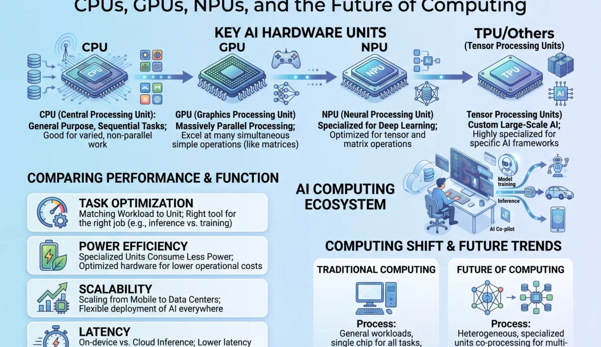
To keep pace, the semiconductor industry has shifted toward specialized AI hardware. Modern computing is no longer defined by a single central chip doing everything. Instead, it relies on a specialized ecosystem of AI processors, encompassing CPUs, GPUs, and NPUs, alongside custom AI chips tailored for high-throughput linear algebra.
This explosive computational demand is not just reshaping microchips—it is redefining physical computing infrastructure, from server racks and high-density networking to direct-to-chip liquid cooling and regional energy grids.
1. The Anatomy of Modern Processors: The Core Triangle
To understand why specialized hardware matters, consider how CPUs, GPUs, and NPUs divide labor inside a modern computer or data center.
THE PROCESSOR COMPARISON AT A GLANCE

       CPU (Central Processing Unit)
       ┌───────────────────────────────┐
       │  [Low Latency / Sequential]   │  • Few powerful cores (4–64)
       │  • Massive cache memory       │  • High clock speeds (3–5+ GHz)
       │  • Complex branch prediction  │  • General-purpose orchestrator
       └───────────────────────────────┘
                       ▲
                       │ Coordinates Tasks
                       ▼
       GPU (Graphics Processing Unit)
       ┌───────────────────────────────┐
       │  [High Throughput / Parallel] │  • Thousands of smaller cores
       │  • Massive memory bandwidth   │  • Optimized for matrix/vector math
       │  • High power draw (300-1000W)│  • Industry standard for training
       └───────────────────────────────┘
                       ▲
                       │ Offloads Sustained Low-Power Inference
                       ▼
       NPU (Neural Processing Unit)
       ┌───────────────────────────────┐
       │  [Specialized / Energy-Lean]  │  • Hardwired MAC/tensor engines
       │  • INT4 / INT8 quantization   │  • Ultra-low power (2–15W)
       │  • Embedded on device silicon │  • Always-on, local AI execution
       └───────────────────────────────┘
2. CPUs: The Master Orchestrators of Computing
The Central Processing Unit (CPU) is the brain of any computing system. Whether it is an Intel Core, an AMD Ryzen, or an ARM-based chip inside a smartphone, the CPU is engineered for versatility and low-latency sequential computing.
CPU ARCHITECTURE: OPTIMIZED FOR SERIAL EXECUTION
┌────────────────────────────────────────────────────────┐
│  Large Control Logic & Out-of-Order Speculation       │
├──────────────┬──────────────┬──────────────┬───────────┤
│ Core 1 (ALU) │ Core 2 (ALU) │ Core 3 (ALU) │ Core 4    │
├──────────────┴──────────────┴──────────────┴───────────┤
│  L1 / L2 Cache Memory                                  │
├────────────────────────────────────────────────────────┤
│  Massive L3 Cache                                      │
├────────────────────────────────────────────────────────┤
│  DRAM Controller (High Latency, Moderate Bandwidth)    │
└────────────────────────────────────────────────────────┘
How CPUs Work
A CPU typically houses between 4 and 64 cores. Each core is an engineering marvel designed to run any instruction set you throw at it:
- High Clock Speeds: Operating at frequencies exceeding 4.0 to 5.0 GHz, CPU cores execute complex instructions in fractions of a nanosecond.
- Large On-Die Caches: CPUs dedicate substantial silicon area to multi-level caches (L1, L2, and L3) to keep critical data immediately adjacent to the arithmetic logic units (ALUs).
- Branch Prediction and Speculative Execution: Modern CPUs guess which pathway an
if/thencode block will follow before the condition has finished evaluating, keeping instruction pipelines full.
Why CPUs Struggle with Heavy AI Workloads
Deep neural networks operate via linear algebra—specifically matrix multiplication ($C = A \times B$). A neural network layer might take an input vector of 4,096 numbers and multiply it by a weight matrix of 4,096 $\times$ 4,096 numbers, requiring tens of millions of discrete multiplications and additions.
A CPU core approaches this sequentially. Even with Vector Extensions (like AVX-512 or AMX), a CPU can only process dozens of numbers per clock cycle. For an application like training an LLM with billions of parameters, a CPU architecture runs into a mathematical wall. It excels at managing the operating system, running game logic, orchestrating database transactions, and parsing business code, but it lacks the parallel pathways needed to crunch matrix calculations at scale.
3. GPUs: The Engines of the AI Revolution
Originally designed to render 3D polygons, shading, and visual pixels for PC gaming, Graphics Processing Units (GPUs) unexpectedly became the foundation of modern artificial intelligence.
GPU vs CPU: PROCESSING PARADIGM

CPU: "A few heavy-duty trucks"         GPU: "Thousands of conveyor belts"
     ┌──────────┐ ┌──────────┐              ┌─┐┌─┐┌─┐┌─┐┌─┐┌─┐┌─┐┌─┐┌─┐┌─┐
     │  Core 1  │ │  Core 2  │              │ ││ ││ ││ ││ ││ ││ ││ ││ ││ │
     └──────────┘ └──────────┘              └─┘└─┘└─┘└─┘└─┘└─┘└─┘└─┘└─┘└─┘
     Moves 4 complex payloads               Moves 10,000 small items
     at 120 mph sequentially.               simultaneously at 35 mph.
The Shift to Parallel Processing
Where a CPU has dozens of powerful cores, a modern enterprise GPU contains tens of thousands of smaller, streamlined cores.
When rendering an image on a 4K display, a GPU calculates the color and lighting for roughly 8.3 million individual pixels simultaneously. Because the color of a pixel on the top-left of your screen rarely depends on a pixel on the bottom-right, this work is “embarrassingly parallel.”
Around 2012, researchers realized that computing the weights and activations of a deep artificial neural network relies on the exact same mathematical operations as rendering 3D graphics: parallel matrix multiplication.
Specialized AI Cores: Tensor and Matrix Accelerators
Modern GPUs designed for AI workloads (such as NVIDIA’s Hopper and Blackwell families, or AMD’s Instinct series) are no longer just graphics processors. They integrate dedicated Tensor Cores:
- Mixed-Precision Arithmetic: Standard computing relies on 32-bit (FP32) or 64-bit (FP64) floating-point numbers. Tensor Cores execute fused multiply-accumulate (FMA) instructions at 16-bit (FP16, BF16) and 8-bit (FP8) precisions, quadrupling computation speeds while slashing memory pressure.
- Massive High-Bandwidth Memory (HBM): GPUs are bound by how quickly they can fetch data. Modern AI processors are packaged with High Bandwidth Memory (such as HBM3e) stacked directly on top of the silicon interposer, delivering multi-terabyte-per-second memory bandwidth.
+--------------------+-----------------------------+-----------------------------+
| Feature            | Central Processing Unit     | Graphics Processing Unit    |
+--------------------+-----------------------------+-----------------------------+
| Core Architecture  | 4 to 64 large cores         | 5,000 to 20,000+ tiny cores |
| Optimized For      | Low-latency sequential code | High-throughput parallelism |
| Clock Speed        | 3.5 GHz – 5.5 GHz           | 1.2 GHz – 2.5 GHz           |
| Memory Bandwidth   | ~50 to 100 GB/s (DDR5)      | ~1,000 to 8,000+ GB/s (HBM) |
| Best AI Role       | Pipeline orchestration, RAG | Model training, heavy batch |
|                    | preprocessing, OS logic     | inference and generation    |
+--------------------+-----------------------------+-----------------------------+
4. NPUs: Dedicated Efficiency for the Edge
If GPUs are so effective, why not run them everywhere?
The answer comes down to power consumption and thermal limits. An enterprise AI GPU draws between 700 and 1,200 watts under full load, generating massive amounts of heat. Even mobile GPUs inside laptops consume 50 to 140 watts, which rapidly drains battery life.
Enter the Neural Processing Unit (NPU)—also referred to as a Neural Engine, AI Accelerator, or Tensor Processing Unit (TPU).
NPU ARCHITECTURE: THE SYSTOLIC ARRAY
              Weights Preloaded
              ┌───┬───┬───┬───┐
Inputs ──────►│MAC│MAC│MAC│MAC│
Stream In     ├───┼───┼───┼───┤
              │MAC│MAC│MAC│MAC│ ──► Continuous Accumulator Outputs
              ├───┼───┼───┼───┤     (Data flows like blood through tissue)
              │MAC│MAC│MAC│MAC│
              └───┴───┴───┴───┘
               * Zero register/cache round-trips during calculation
               * Extreme energy efficiency (Milliwatts to few Watts)
How NPUs Achieve Extreme Efficiency
An NPU is an Application-Specific Integrated Circuit (ASIC) custom-built for one job: running trained neural networks using minimal power.
- Systolic Arrays: In a standard CPU or GPU, every calculation requires fetching data from a register or cache, running the math, and writing the result back. NPUs often use systolic arrays—grids of Multiply-Accumulate (MAC) units where data flows directly from one calculating cell to the next without constantly reading and writing to memory.
- Aggressive Quantization (INT8 & INT4): While training an AI model requires high floating-point precision, running an already-trained model (inference) can be executed using low-precision 8-bit or 4-bit integers. NPUs are hardwired to execute these low-bit integer operations at lightning speeds.
- Low-Power Profile: While a desktop GPU pulls hundreds of watts, an on-device NPU performs trillions of operations per second while drawing only 2 to 10 watts.
This efficiency is why NPUs are embedded across consumer silicon—from Apple’s A-series and M-series chips to Qualcomm Snapdragon X Elite, Intel Core Ultra, and AMD Ryzen AI processors. They handle continuous, background AI tasks (such as webcam eye contact, real-time voice transcription, background noise cancellation, and photo enhancement) without draining your battery or causing the cooling fans to roar.
5. Summary Matrix: CPU vs. GPU vs. NPU
┌────────────────────────────────────────────────────────────────────────┐
│                   PROCESSOR CHARACTERISTICS MATRIX                     │
├──────────────┬──────────────────┬──────────────────┬───────────────────┤
│ Metric       │ CPU              │ GPU              │ NPU               │
├──────────────┼──────────────────┼──────────────────┼───────────────────┤
│ Core Count   │ Few (Tens)       │ High (Thousands) │ Dedicated Array   │
├──────────────┼──────────────────┼──────────────────┼───────────────────┤
│ Task Scope   │ General Purpose  │ Graphics & Math  │ Pure AI Inference │
├──────────────┼──────────────────┼──────────────────┼───────────────────┤
│ Latency      │ Ultra-Low        │ Moderate         │ Low to Moderate   │
├──────────────┼──────────────────┼──────────────────┼───────────────────┤
│ Throughput   │ Low              │ Massive          │ High (Optimized)  │
├──────────────┼──────────────────┼──────────────────┼───────────────────┤
│ Power Draw   │ 15W – 300W       │ 100W – 1000W+    │ 1W – 25W          │
├──────────────┼──────────────────┼──────────────────┼───────────────────┤
│ Primary Role │ System Orchestr. │ Training & Heavy │ On-Device / Edge  │
│              │ & General Logic  │ Scaled Inference │ Efficient Tasks   │
└──────────────┴──────────────────┴──────────────────┴───────────────────┘
6. How AI Is Reshaping Data Centers and Physical Infrastructure
The impact of AI hardware extends far beyond silicon dies. The sheer physical density and power draw of AI processors have fundamentally broken traditional enterprise data center architecture.
THE DATA CENTER EVOLUTION

Traditional Web Data Center:
[Air Handling Units] ──► Air Blowers ──► 5kW to 15kW Server Racks ──► Exhaust
* Relies on circulating ambient cold air.

Modern AI Supercomputing Cluster:
[Fluid Distribution Unit] ──► Coolant Loops ──► 40kW to 100kW+ Racks
                                                    │
                                                    ├─► Direct-to-Chip Cold Plates
                                                    ├─► Optical Interconnect Fabrics
                                                    └─► 800Gbps+ Lossless RoCE/InfiniBand
The Death of Air Cooling: The Rise of Liquid Systems
For thirty years, data centers kept hardware cool by pumping cold air through raised floors and server aisles. This method works well for standard servers drawing 5 to 15 kilowatts (kW) per rack.
Modern AI compute racks, however, concentrate dozens of power-hungry AI accelerators into compact spaces, pushing power densities to 40kW, 80kW, and well over 100kW per individual rack. Air simply does not possess the thermal heat capacity to cool silicon operating at these thermal densities.
As a result, high-density facilities are transitioning to liquid cooling:
- Direct-to-Chip (Cold Plate) Cooling: Closed loops circulate dielectric fluid or treated water directly across micro-channeled copper plates bolted to the GPU and CPU heat spreaders, pulling heat directly from the chip package.
- Immersion Cooling: Entire server blades are submerged in non-conductive, dielectric fluid tanks that absorb heat via phase changes or liquid circulation.
- Chilled Water Distribution Units (CDUs): Heavy-duty pumping stations manage coolant flow and heat exchange at the row and facility level.
The AI Networking Bottleneck: Moving Trillions of Parameters
In an AI cluster, training a frontier model requires distributing billions of parameters across thousands of GPUs working in sync. If one GPU completes its layer calculation and has to wait 5 milliseconds for surrounding nodes to synchronize their gradients, the entire multi-million-dollar cluster stalls.
To eliminate these networking choke points, AI clusters use specialized, low-latency networking fabrics:
- InfiniBand and RoCEv2 (RDMA over Converged Ethernet): Protocols that allow GPUs on different servers to read and write directly to each other’s memory buffers (Remote Direct Memory Access) without routing data through the operating system or CPU network stack.
- Ultra-High Bandwidth: Data centers are actively standardizing on 800 Gbps and 1.6 Tbps networking switches and optical transceivers to prevent cluster interconnect starvation.
CLUSTER DISTRIBUTED MEMORY ACCESS:
[Server Node 1: GPU] ──► Direct Memory Read (RDMA) ──► [Server Node 2: GPU]
                      ▲                               ▲
                      └────── Bypasses OS & CPU ──────┘
                             (Sub-microsecond latency)
Energy Grids and Infrastructure Siting
A modern hyperscale AI data center campus can demand between 500 megawatts and over a gigawatt (GW) of electrical capacity—equivalent to the power consumption of a mid-sized metropolitan city.
This energy appetite is reshaping where infrastructure is constructed. Tech companies no longer pick data center locations solely based on proximity to major internet exchanges or financial centers. Instead, facilities are being built next to abundant energy sources: hydroelectric plants, nuclear power stations, and dedicated utility-scale solar and battery installations to satisfy compute demands sustainably.
7. The Future of Computing: What Comes Next?
As silicon fabrication approaches the physical atomic boundaries of silicon dioxide gates, chip designers are deploying novel paradigms to sustain computational progress:
FRONTIERS IN NEXT-GENERATION AI HARDWARE

1. Advanced Packaging:
   [HBM3e Stack] ──► [Silicon Interposer (CoWoS)] ◄── [Compute Chiplets]
   * Modular chiplets replace monolithic silicon dies.

2. Silicon Photonics:
   [Electronic Logic] ──► Photonic Micro-Rings ──► Optical Fiber Pulse
   * Light replaces copper traces for chip-to-chip data transfer.

3. Neuromorphic Computing:
   [Artificial Spiking Neurons] ──► Event-Driven Activation
   * Mimics biological brains: consumes power only when a signal fires.
1. Chiplets and Advanced 2.5D/3D Packaging
Fabricating a single, massive silicon die (monolithic architecture) is hitting the “reticle limit”—the physical size threshold a photolithography machine can expose onto a wafer. Defects in giant dies also result in low manufacturing yields.
The industry has pivoted to chiplets. Using advanced packaging technologies (such as TSMC’s CoWoS—Chip-on-Wafer-on-Substrate), manufacturers build smaller, modular dies (separating compute, memory, and I/O) and stitch them together on a microscopic silicon interposer with tens of thousands of microscopic connections. This modular approach allows chips to behave as a single coherent processor while drastically cutting manufacturing costs and maximizing yields.
2. Optical Interconnects and Silicon Photonics
Copper wires struggle at multi-terabit bandwidths: they generate heat, suffer from electromagnetic crosstalk, and degrade signals over distances as short as a few centimeters.
Silicon photonics replaces electrical signals on copper traces with laser pulses transmitted through microscopic optical waveguides etched directly into the silicon packaging. By moving data using light rather than electricity, optical interconnects reduce interconnect energy consumption by up to 80% while enabling sub-nanosecond data transfers between processors.
3. Neuromorphic and Analog In-Memory Computing
Traditional computers follow the von Neumann architecture: computing (ALU) and storage (Memory) are physically separated, wasting immense energy shuttling data back and forth across the memory bus.
In-Memory Computing integrates memory and processing together. Using resistive RAM (ReRAM) or memristors, these chips adjust electrical resistance to execute matrix math directly inside the memory array, performing linear algebra using analog physics rather than digital logic.
Meanwhile, Neuromorphic chips mimic the human brain’s architecture. Instead of processing continuous clock cycles, they use event-driven “spiking” neural networks that consume power only when a neuron fires—promising a 100x leap in energy efficiency for edge sensors and robotics.
The Hardware Paradigm Shift
The artificial intelligence revolution is fundamentally a hardware story.
Algorithms like backpropagation and neural attention mechanisms existed in academic literature for years. What ignited modern AI was the convergence of those algorithms with specialized silicon architectures capable of crunching parallel linear algebra at unprecedented scale.
As computing enters this era:
- The CPU remains the essential orchestrator, managing system state, low-latency branching, and sequential application logic.
- The GPU serves as the parallel computing workhorse, driving deep learning model training and scaled batch inference in data centers worldwide.
- The NPU brings energy-efficient intelligence to consumer devices, enabling privacy-preserving, always-on AI at the edge.
Understanding these foundational differences is key to navigating the modern tech ecosystem. The future of computing is no longer about making single processors run faster—it is about orchestrating specialized silicon architectures, rethinking physical data centers, and scaling the infrastructure that powers artificial intelligence from the data center to your pocket.
For a deeper technical conversation on how the underlying semiconductor architecture works, you can check out this discussion on how CPUs, GPUs, and NPUs work. This video explores the architectural differences between processors and the engineering challenges behind next-generation AI silicon.
