

 By
By The smartphone is no longer just a handheld telecommunication device; it has become the most concentrated showcase of modern computing, material science, and computational physics. For years, mobile updates followed a predictable, iterative cycle: fractional processor speed bumps, marginally slimmer bezels, and minor camera pixel increases.
Today, that period of incremental progress has been replaced by a transformative leap in smartphone technology. Handset architectures are shifting under pressure from compute-heavy artificial intelligence workloads, demanding graphical pipelines, multi-fold form factors, and non-terrestrial satellite communication.
From 3-nanometer and sub-3nm mobile systems-on-chip (SoCs) equipped with specialized neural engines to high-density silicon-carbon batteries, variable-aperture periscope optics, and tandem OLED panels, the latest smartphone features reflect significant engineering advancements.
This comprehensive guide analyzes modern mobile technology, detailing the architectural breakthroughs across processors, camera pipelines, on-device AI, display materials, satellite connectivity, and electrochemical battery developments defining current smartphone trends.
1. Processors & Silicon Architecture: The 3nm Era and Custom Microarchitectures
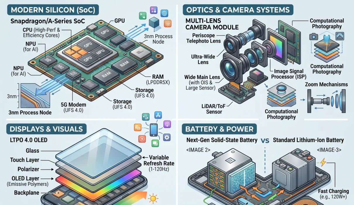
The modern System-on-Chip (SoC) integrates the Central Processing Unit (CPU), Graphics Processing Unit (GPU), Neural Processing Unit (NPU), Image Signal Processor (ISP), and 5G/Satellite modem onto a single silicon die. Modern fabrication relies on extreme ultraviolet (EUV) photolithography, yielding nodes at 3nm and below (such as TSMC’s N3E and N3P processes, as well as gate-all-around GAA / nanosheet architectures).
THE MODERN MOBILE SYSTEM-ON-CHIP (SoC) COMPONENT TOPOLOGY:

[ Custom Prime & Efficiency CPU Cores ] <───► [ High-Bandwidth Unified Memory LPDDR5X / 6 ]
                       ▲
                       │ Ultra-Low Latency Interconnect Fabric
                       ▼
[ Neural Processing Unit (NPU) ]        <───► [ ISP: Neural Multi-Exposure Raw Pipeline ]
                       ▲
                       │
                       ▼
[ Hardware Ray Tracing GPU Engine ]     <───► [ Integrated Sub-6GHz / mmWave / NTN Modem ]
The Transition Away from Stock Arm Reference Designs
A primary trend in flagship mobile silicon is the move toward custom CPU core microarchitectures.
Rather than deploying standard off-the-shelf Arm Cortex CPU designs, chipmakers are engineering proprietary core layouts:
- Custom Prime Cores: High-frequency, large-out-of-order execution windows with expanded L1 and L2 caches, running clock speeds above 4.0 GHz to 4.3 GHz.
- All-Big Core Architectures: High-tier processors have largely eliminated traditional ultra-low-power “efficiency-only” cores (like the Cortex-A55). Instead, mobile silicon deploys a cluster composed entirely of high-performance prime cores and mid-range performance cores. Under light operational loads, these performance cores run at low voltage and frequency, delivering higher IPC (instructions per cycle) and completing background workloads faster to return to an idle sleep state, improving battery consumption.
Hardware-Accelerated Ray Tracing and Mesh Shading
Mobile GPUs are engineered to execute console-tier rendering techniques on sub-10-watt power envelopes:
- Dedicated BVH Traversal Hardware: Dedicated ray-tracing accelerators calculate Bounding Volume Hierarchy (BVH) intersections directly in silicon rather than offloading math to software shaders.
- Global Illumination & Refraction: Mobile titles render realistic real-time reflections, dynamic contact shadows, and ambient light bounces at native refresh rates with the aid of temporal upscaling algorithms.
- Mesh Shading Pipelines: Geometry pipelines allow dynamic level-of-detail adjustments, rendering scenes with millions of polygons without stalling the geometry engine.
2. On-Device AI & Neural Processing Units (NPUs)
While early artificial intelligence in mobile devices relied on offloading data to cloud-based servers, contemporary mobile technology prioritizes local, on-device neural execution.
+---------------------------+-----------------------------------+------------------------------------------+
| Processing Model          | Advantages                        | Limitations                              |
+---------------------------+-----------------------------------+------------------------------------------+
| **Cloud-Based AI**        | Access to trillion-parameter      | High latency; requires active internet;  |
|                           | foundational models               | privacy/data-transmission vulnerabilities|
+---------------------------+-----------------------------------+------------------------------------------+
| **On-Device Edge AI**     | Sub-50ms latency; zero data leaves| Constrained by device thermal envelope   |
| (Modern Flagships)        | handset; operates 100% offline    | and system RAM memory bandwidth          |
+---------------------------+-----------------------------------+------------------------------------------+
| **Hybrid Edge-Cloud**     | Lightweight queries handled locally; | Complex routing logic required to        |
|                           | deep reasoning routed upstream    | balance user experience seamlessly       |
+---------------------------+-----------------------------------+------------------------------------------+
The Mechanics of the Sub-Watt Mobile NPU
Modern NPUs are specialized parallel compute engines designed specifically for matrix multiplications (tensor dot-products) that dominate neural networks.
- Int8 and Int4 Quantization: Large language models (LLMs) with 3 to 7 billion parameters traditionally require tens of gigabytes of floating-point (FP32 or FP16) memory. Edge NPUs leverage 4-bit and 8-bit integer quantization engines, compressing model weights to fit comfortably within 3GB to 5GB of unified mobile RAM without noticeable degradation in reasoning accuracy.
- Transformer Engine Acceleration: Modern NPUs feature dedicated silicon accelerators for the attention mechanisms core to transformer architectures, running local generative voice transcription, live cross-lingual call translation, and contextual text generation at speeds exceeding 20 to 30 tokens per second.
3. Camera Systems: 1-Inch Sensors, Variable Apertures, and Computational Raw
Smartphone optics have evolved beyond the megapixel marketing war. Current innovations focus on physical sensor area, photon collection efficiency, and multi-frame computational synthesis.
THE COMPUTATIONAL CAMERA CAPTURE PIPELINE:

[ Photons hit 1-Inch Type Stacked Sensor ]
                     │
                     ▼
[ 14-Bit Direct Uncompressed RAW Frames Captured into Circular Buffer ]
                     │
       ┌─────────────┴─────────────┐
       ▼                           ▼
[ Semantic Segmentation Engine ]   [ Zero-Shutter-Lag Fusion ]
Identifies skin, hair, sky,        Merges 8–12 underexposed frames
textiles, foliage down to pixel    to eliminate motion blur & recover
boundaries via the NPU             dynamic range without HDR clipping
                     │
                     ▼
[ Demosaicing & Tonemapping Pipeline Output ]
1-Inch-Type Sensors & Two-Layer Transistor Pixels
- Sensor Surface Area: Traditional mobile cameras utilized microscopic 1/2.55-inch sensors. Modern flagships incorporate massive 1-inch-type imaging sensors (such as the Sony LYT-900 series). A larger physical surface area captures dramatically more natural light, creating shallow optical depth-of-field (genuine background bokeh) and a higher signal-to-noise ratio in low-light environments.
- Stacked Two-Layer Transistor Pixels: Conventional CMOS sensors place the photodiode and its control pixel transistor on the same silicon plane. Modern stacked sensors separate the photodiode layer onto an upper tier, placing the transistor circuitry beneath it. This effectively doubles the light-gathering capacity of each individual pixel, preventing highlight blowout and shadow clipping in high-contrast scenes.
Periscope Optical Telephotos with Floating Prism Groups
Zooming without sacrificing chassis thickness requires folding the optical axis horizontally inside the phone:
- Periscope Prisms: A 90-degree reflective prism directs light along the length of the smartphone’s chassis through a multi-element motorized lens barrel to a recessed sensor.
- Floating Focus Elements: Modern telephotos move optical groups internally. This allows a single lens to shift between serving as a 3.5x to 5x optical portrait zoom and moving forward to focus on micro-subjects just centimeters away, executing telephoto macro photography with creamy optical blur.
+------------------------+------------------------------------+------------------------------------------+
| Optical Component      | Mechanism                          | Consumer Photography Impact              |
+------------------------+------------------------------------+------------------------------------------+
| **Physical Step-Aperture**| Mechanical dual-blade or multi-  | Controls depth-of-field optically;       |
|                        | blade iris (e.g., f/1.4 to f/4.0)  | eliminates edge fringing in landscape    |
+------------------------+------------------------------------+------------------------------------------+
| **Sensor-Shift OIS**   | Actuators physically shift the CMOS| Compensates for hand tremor up to 5°;    |
|                        | sensor along X, Y, and Z axes      | keeps night exposures tack-sharp         |
+------------------------+------------------------------------+------------------------------------------+
| **Prism Periscope**    | Horizontally aligned optical barrel| True 5x–10x optical magnification without|
|                        | inside the smartphone body         | camera module protrusion                 |
+------------------------+------------------------------------+------------------------------------------+
4. Display Technology: Tandem OLEDs, LTPO 4.0, and Multi-Fold Form Factors
The display remains the primary sensory interface of the smartphone, and recent engineering focuses on outdoor visibility, energy conservation, and flexible structural integrity.
TANDEM OLED DISPLAY STACK ARCHITECTURE:

   [ Surface Cover Glass: Ceramic / Anti-Reflective Coating ]
   [ Polarizing / CoE (Color on Encapsulation) Layer ]
   [ Upper Light-Emitting OLED Organic Layer (RGB) ]
   ────────────────────────────────────────────────────────
   [ Intermediate Charge Generation Layer (CGL) ]  <--- Multiplies photon yield
   ────────────────────────────────────────────────────────
   [ Lower Light-Emitting OLED Organic Layer (RGB) ]
   [ Low-Temperature Polycrystalline Oxide (LTPO) Backplane ]
Tandem OLED Architecture
Traditional single-layer OLEDs degrade rapidly if driven at continuous ultra-high current densities. Modern flagship displays adopt Tandem OLED structures:
- Dual Stacked Emissive Layers: By stacking two organic light-emitting layers in series with a Charge Generation Layer (CGL) in between, the panel produces double the light output for the same electrical current—or delivers standard brightness at vastly lower power consumption.
- Peak Brightness Frontiers: Tandem OLED panels achieve localized HDR highlights exceeding 4,500 to 5,000 nits, allowing displays to remain readable under direct, unfiltered mid-day sunlight.
- Longevity: Because each layer is driven at lower voltage to reach a given luminance, pixel burn-in rates drop by up to 50% compared to traditional single-stack OLED panels.
Variable Refresh Rate via LTPO 4.0
Low-Temperature Polycrystalline Oxide (LTPO) backplanes allow dynamic refresh switching:
- Dynamic 1Hz to 120Hz/144Hz Transitions: When reading a static book or viewing an Always-On Display (AOD), the panel downclocks to an imperceptible 1 frame per second (1Hz), drastically reducing battery draw. The millisecond a finger touches the glass, the backplane ramps up to 120Hz or 144Hz for fluid scrolling.
Form Factor Evolution: Foldables and Tri-Folds
The structural design of mobile devices is diversifying:
- Waterdrop Hinge Mechanics: Modern foldables utilize multi-link teardrop hinges. When closed, the flexible display loops backward inside the hinge chassis in a teardrop curve, eliminating the inner gap, protecting against dust intrusion, and virtually flattening the visible screen crease.
- Tri-Fold Architectural Expansion: Dual-hinge, Z-fold devices fold outward and inward, functioning as a standard 6.5-inch phone in single-screen mode while opening outward to form a seamless 10-to-11-inch continuous OLED tablet.
5. Battery & Power: The Silicon-Carbon Revolution and Thermal Management
Battery technology has long been the primary bottleneck in mobile computing. For decades, manufacturers relied on standard graphite anodes, hitting a ceiling around 5,000mAh for standard smartphone chassis dimensions. The widespread adoption of silicon-carbon (Si/C) composite anodes has transformed energy density.
THE ANODE REVOLUTION:

CONVENTIONAL GRAPHITE ANODE:
• Lithium storage capacity: ~372 mAh/g
• Maximum phone capacity in 8.2mm chassis: ~4,800 - 5,000 mAh
• Slower initial high-current acceptance

SILICON-CARBON COMPOSITE ANODE (10% - 30% Silicon Content):
• Theoretical silicon capacity: ~4,200 mAh/g
• Pack-level density: Exceeds 800 Wh/L
• Capacity in sub-8.5mm chassis: 6,000 mAh to 7,500+ mAh
• Superior low-temperature performance (-20°C retention)
Why Silicon-Carbon Transforms Mobile Endurance
- Energy Density: Silicon can bind significantly more lithium ions by weight than graphite. By blending engineered nano-porous silicon structures into carbon matrices, battery cells achieve volumetric densities exceeding 800 to 850 Wh/L. This allows manufacturers to pack 6,000mAh to 7,000mAh into thin, light bodies that previously topped out at 5,000mAh.
- High-Rate Fast Charging (80W–120W): Silicon structures accept lithium ions rapidly during early charging phases, allowing 6,500mAh batteries to charge from 1% to 100% in under 30 minutes without generating dangerous heat spikes.
- Cycle Life Engineering: Because pure silicon expands by up to 300% when absorbing lithium (which can crack electrode surfaces), modern cells employ carbon-coated nano-silicon clusters and specialized elastic polymer binders to maintain cell integrity across 1,200 to 1,600 full charge cycles.
6. Connectivity: Non-Terrestrial Satellite Networks, Wi-Fi 7, and 5G-Advanced
Connectivity standards now ensure reliable data transmission whether you are standing in a crowded stadium or hiking through an isolated mountain range.
+---------------------------+-----------------------------------+------------------------------------------+
| Standard                  | Technical Specification           | Real-World User Benefit                  |
+---------------------------+-----------------------------------+------------------------------------------+
| **Direct-to-Cell NTN**    | 3GPP Rel-17/18 Satellite Protocol;| Emergency SOS, bidirectional text,       |
| (Satellite Connectivity)  | L-band & S-band RF transceivers   | and location sharing with zero cell towers|
+---------------------------+-----------------------------------+------------------------------------------+
| **Wi-Fi 7 (802.11be)**    | 320 MHz channels, 4096-QAM,       | Throughputs up to 46 Gbps; sub-millisecond|
|                           | Multi-Link Operation (MLO)        | wireless latency for cloud gaming/VR     |
+---------------------------+-----------------------------------+------------------------------------------+
| **5G-Advanced (5.5G)**    | 10x uplink capacity, L4S latency, | Stable connectivity in dense crowds;     |
|                           | RedCap IoT protocol support       | extended battery life during 5G download |
+---------------------------+-----------------------------------+------------------------------------------+
Direct-to-Cell Satellite Connectivity
Handsets now incorporate specialized RF front-end components and high-gain antenna arrays that communicate directly with low-Earth-orbit (LEO) satellite constellations orbiting 500 miles above Earth:
- Bidirectional Emergency Telemetry: When beyond the reach of terrestrial cell towers, smartphones send emergency text messages, GPS coordinates, and medical IDs directly via satellite.
- Satellite Voice & Messaging: Advanced networks support two-way non-emergency SMS and compressed voice notes without requiring external antenna accessories.
Wi-Fi 7 and Multi-Link Operation (MLO)
The rollout of Wi-Fi 7 (802.11be) solves congested home and office network bottlenecks:
- Multi-Link Operation (MLO): Traditional devices connect to a single wireless band (either 2.4 GHz, 5 GHz, or 6 GHz). Wi-Fi 7 smartphones transmit and receive data across multiple bands simultaneously. If interference interrupts the 6 GHz band, packets route instantaneously over the 5 GHz band without dropping connections or lagging.
- 4096-QAM: Transmits 20% more data per symbol than Wi-Fi 6, maximizing multi-gigabit fiber connections throughout modern homes.
7. Materials, Durability, and Structural Engineering
As internal hardware becomes more sophisticated, exterior chassis materials must provide rigid thermal dissipation and structural protection.
THE EXTERIOR DURABILITY STACK:

[ Screen Layer ]       Ceramic-infused nanocrystal glass (Anti-reflective, scratch resistant)
                                   │
[ Armor Chassis ]      Grade 5 Titanium / Aerospace Aluminum alloy (High strength-to-weight)
                                   │
[ Thermal Core ]       Dual-circulation 3D Vapor Chamber with capillary wick structure
                                   │
[ Ingress Barrier ]    IP68 / IP69 Hermetic Gasket Sealing (Resists high-pressure hot water jets)
- Grade 5 Titanium & Bio-Alloys: High-end flagships incorporate Grade 5 Titanium (Ti-6Al-4V) bonded to an aluminum inner substructure via solid-state diffusion bonding. This combination provides high tensile strength, lowers overall device weight, and dissipates heat effectively away from the mainboard.
- IP68 and IP69 Ingress Protection: Leading flagships have graduated from standard IP68 submersion ratings to IP69. An IP69 rating certifies that the smartphone’s hermetic acoustic mesh, charging port, and button seals resist high-pressure, high-temperature water jets (up to 80°C / 176°F at 100 bar pressure), protecting against accidental drops into hot tubs or industrial washdowns.
- Large-Scale Vapor Chamber Cooling: High-performance silicon draws substantial power under sustained workloads. Smartphones integrate capillary 3D vapor chambers with dual-channel fluid circulation covering both the SoC and the battery pack, preventing thermal throttling during extended 4K video recording or intensive gaming sessions.
The Smartphone Technology Horizon: What to Expect Next
Smartphone engineering has reached an inflection point where software, artificial intelligence, and physical hardware operate as an integrated system. We have moved beyond superficial specification races into an era of meaningful capability:
- Batteries that reliably last two full days through high-density silicon-carbon chemistry.
- Cameras that capture true optical depth and light fidelity through 1-inch stacked sensors and variable mechanical irises.
- Displays that fold, slide, and adapt from pocketable phones into full-scale workstations with zero crease degradation.
- Silicon that reasons privately on your device without sending personal context to remote cloud servers.
As the smartphone continues to incorporate advanced spatial audio, non-terrestrial satellite links, and multimodal intelligence, it solidifies its position as the primary computational hub of modern life.